Intel CPU generation list – Core i-series and beyond

Table of Contents
How long has the Intel CPU generation list been? In a nutshell, the Intel Core i-series has now become a household name worldwide. The company has been at the forefront of processor technology for decades. Moreover, Intel’s CPUs have played a pivotal role in shaping the digital landscape. However, all of these didn't happen over a year or two.
Over the years, Intel has introduced numerous CPU generations, each more advanced than the last. In this article, we will take you on a journey through Intel’s Core i-series CPU generation list.
What are Intel generations?
Intel generations refer to the various iterations or releases of Intel’s central processing units (CPUs). These CPU generations represent a series of incremental advancements in processor technology and architecture.
Each generation typically features improvements in performance, power efficiency, and the integration of new features. Intel uses codenames for these generations. These codenames are often associated with a specific microarchitecture. We will go through each Intel generation CPU of the Core i-series. Additionally, we will also look at the most significant architecture and feature changes in them.
Intel Core i-series CPU generations list
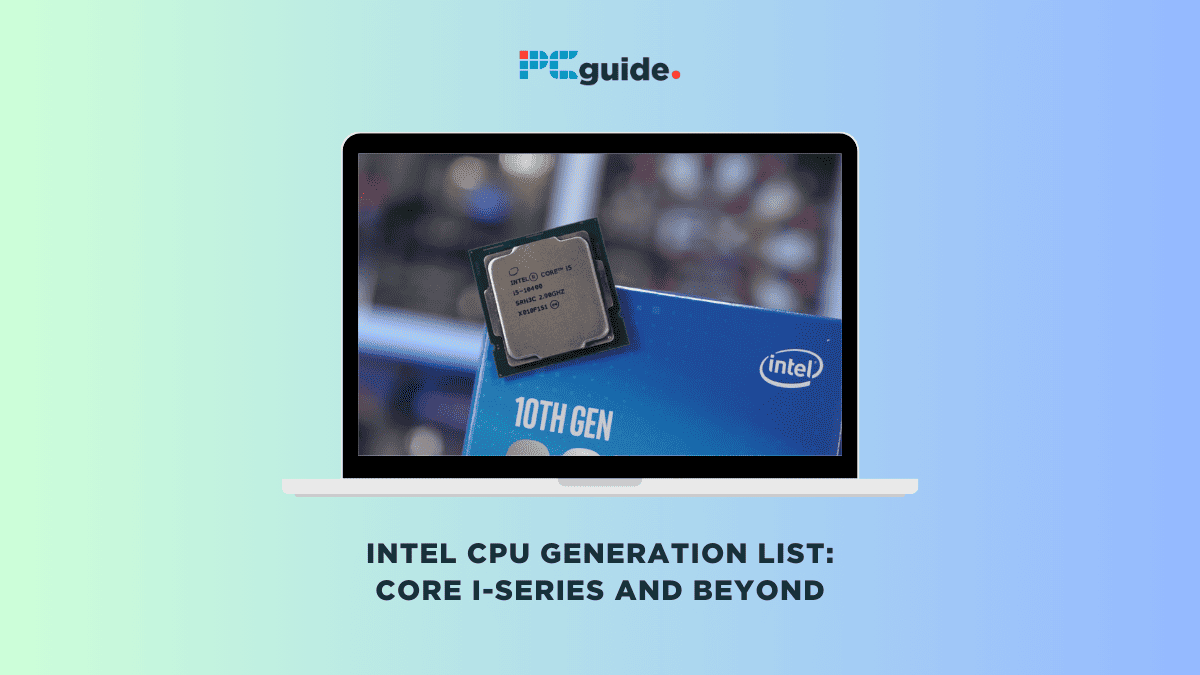
There have been a total of 14 Intel generations until now. Intel has also revealed some details of the two upcoming generations, their codenames, and basic features. Let's look at each one of the Intl Core i-series CPU generations.
Intel 1st gen Core i-series CPUs – Nehalem
Nehalem was the codename of Intel's 1st gen Core i-series processors. It was introduced in 2008 and was based on 45 nm microarchitecture. It marked a significant departure from its predecessors, particularly the Core 2 Duo.
The execution engine, largely retained from Core 2, was optimized for efficiency, while the emphasis was placed on improving data and code throughput by widening communication channels. Simultaneous multithreading (SMT) made a return to Intel’s mainstream processors, boosting system bandwidth and keeping execution units busier.
To accommodate the increased flow, Nehalem increased buffer sizes. Some increased buffer sizes were the reorder buffer, reservation station, load, and store buffers. This increase ensured more efficient resource utilization.
Intel 2ndth gen Core i-series CPUs – Sandy Bridge
The second generation of Intel Core i-series processors was code-named Sandy Bridge. One of the notable architectural changes was the introduction of a ring bus. It is a communication system that interconnects all resources, including CPU and graphics cores, via over 1,000 on-chip wires.
It can operate at impressive speeds of 96Gbps with a 3GHz clock. This makes it remarkably versatile in reconfiguring chip designs for various applications. While retaining Hyper-Threading, which transforms a physical core into two virtual cores, Sandy Bridge introduces an enhanced Turbo Boost feature.
This enhancement allowed all cores to overclock simultaneously for short bursts when the chip was running cool. This procedure allowed the effective use of the chip’s substrate as a heatsink.
Additionally, Sandy Bridge introduced Advanced Vector Extensions (AVX), which widens the vector width from 128 to 256 bits. Thus, it promises a doubling of floating-point performance, particularly benefiting video processing tasks.
Furthermore, Sandy Bridge incorporates AES New Instructions (AESNI) to accelerate hardware-based encryption. Regarding servers, Intel planned to introduce server chips based on the Sandy Bridge architecture in 2011, while Ivy Bridge, a 22nm ‘tick’ version, was expected to arrive by the end of 2012.
Notably, Sandy Bridge introduced a new socket, LGA 1155, with one fewer pin than its predecessor Nehalem. This necessitated new motherboard designs. While offering increased performance, this architectural change rendered compatibility with existing motherboards unfeasible.
Intel 3rd gen Core i-series CPUs – Ivy Bridge
Released in 2012, Intel's 3rd generation Core i-series processors were code-named Ivy Bridge. They were built on a 22nm manufacturing process and introduced several noteworthy changes over their 2nd generation predecessors, the Sandy Bridge processors. The most significant shift was the move from a 32nm to a 22nm process technology, which allowed for better power efficiency and improved performance.
Ivy Bridge processors utilized the new 22nm Tri-Gate transistors, which brought enhancements in energy efficiency and allowed for more transistors to be packed into a smaller space. This microarchitecture, known as the “Tick” in Intel’s “Tick-Tock” development cycle, laid the foundation for Ivy Bridge’s improved performance and power efficiency.
In terms of the physical socket, Ivy Bridge processors still used the LGA 1155 socket, similar to Sandy Bridge, ensuring compatibility with existing motherboards. This was a convenient upgrade for those looking to upgrade without overhauling their entire system.
In terms of performance, Ivy Bridge processors showcased a 3% to 6% increase in CPU performance when compared clock for a clock with their Sandy Bridge counterparts. This increase was due to architectural refinements and the smaller transistor size.
Moreover, Ivy Bridge processors also delivered a substantial boost in integrated GPU performance. They offered a potential 25% to 68% increase compared to Sandy Bridge. Therefore, they were more capable of graphics-intensive tasks, multimedia, and even light gaming.
Intel 4th gen Core i-series CPUs – Haswell
Intel’s 4th generation processors, codenamed Haswell, showed the biggest leap in microarchitecture and performance at the time. These processors were officially announced by Intel in June 2013 and brought a host of new features and improvements over the 3rd generation Ivy Bridge processors.
Haswell utilized 22 nm microarchitecture. It introduced low-power processors designed for convertible or “hybrid” ultrabooks, denoted by the “U” suffix. Haswell processors were used with the Intel 8 Series chipsets, Intel 9 Series chipsets, and Intel C220 series chipsets. The processors stick to the same LGA 1150 socket.
Compared to Ivy Bridge, Haswell processors offered notable performance enhancements, including:
- Approximately 8% faster vector processing.
- Up to 5% higher single-threaded performance.
- 6% higher multi-threaded performance.
- Haswell’s integrated GPU showed up to a 20% performance increase over Ivy Bridge’s integrated GPU.
- Overall, Haswell demonstrated an average total performance improvement of about 3%.
- However, desktop variants of Haswell drew between 8% and 23% more power under load than Ivy Bridge, making power efficiency an important consideration.
Haswell also introduced several new features. Some of the most prominent features included:
- Fully Integrated Voltage Regulator (FIVR): Some components were moved from the motherboard to the CPU, enhancing power management and efficiency.
- New instructions, including Advanced Vector Extensions 2 (AVX2), gather, BMI1, BMI2, ABM, and FMA3 support.
- Intel Transactional Synchronization Extensions (TSX) for certain Haswell variants, although there were early issues that led to disabling this feature in some CPUs.
- Advanced power-saving features, such as low-power C6 and C7 sleep states, necessitate compatible power supply units (PSUs).
- Enhanced graphics support for Direct3D 11.1 and OpenGL 4.3.
- Different versions of the integrated GPU, including GT1, GT2, GT3, and GT3e with 40 execution units and embedded DRAM (eDRAM).
Intel 4th-generation processors featured some of the best LDA 1150 socket chips. Two among them, the Core i7-4790 and Core i5-4690, were the most popular ones.
Intel 5th gen Core i-series CPUs – Broadwell
Intel’s 5th generation processors were code-named Broadwell and released in 2015. These processors were designed with a focus on improved performance, energy efficiency, and enhanced integrated graphics. There were three major design variants released for Broadwell processors:
- Broadwell-Y: These processors were designed as a system-on-a-chip (SoC) with low thermal design power (TDP) of 4.5 W and 3.5 W, making them suitable for tablets and specific ultrabook-class devices. They featured GT2 GPUs and supported up to 8 GB of LPDDR3-1600 memory.
- Broadwell-U: Targeted for ultrabooks and NUC platforms, Broadwell-U processors came in two TDP classes, 15 W and 28 W. They were designed for motherboards with the PCH-LP chipset and supported up to 16 GB of DDR3 or LPDDR3 memory. These processors offered 2+2 and 2+3 configurations with varying GPU options.
- Broadwell-H: With TDP classes of 37 W and 47 W, these processors were designed for various form factors, including mini-ITX motherboards and all-in-one systems. They were available in both single and dual-chip configurations, with GT3e and GT2 GPUs, and supported up to 32 GB of DDR3-1600 memory.
Here are some of the new features introduced in this next-gen processor:
- Video Decoding and Encoding: Broadwell processors introduced significant improvements to Intel Quick Sync Video, adding support for VP8 hardware decoding and encoding. They also brought support for VP9 and HEVC 10-bit decoding through the integrated GPU. HEVC decode was achieved through a combination of the fixed-function video decoder and shaders.
- Graphics Enhancements: Broadwell’s integrated GPU supported Direct3D 11.2, OpenGL 4.4 (4.5 on Linux), and OpenCL 2.0, enhancing graphics capabilities for gaming and multimedia applications. It was marketed as Direct3D-12-ready, preparing for future graphics APIs.
- Intel Turbo Boost Max Technology 3.0: Introduced in Broadwell-E processors, this technology identified the processor’s fastest core and directed critical workloads to it, optimizing performance for single-threaded applications.
Intel 6th gen Core i-series CPUs – Skylake
The next generation of the Intel Core i-series processors was code-named Skylake. Skylake processors used the LGA 1151 socket for mainstream desktop processors, and the enthusiast gaming/workstation X-series processors used the LGA 2066 socket.
Skylake represented a microarchitecture redesign, maintaining the 14 nm manufacturing process technology used in the previous generation, Broadwell. The removal of the fully integrated voltage regulator (FIVR) was a notable change from the Haswell architecture. Voltage regulation was moved back to the motherboard. Skylake also introduced Direct Media Interface (DMI) 3.0, which allowed for higher speeds of up to 8 GT/s compared to DMI 2.0.
Here are some improvements made in terms of new features introduced in this generation:
- CPU improvements included a deeper out-of-order buffer, improved execution units, more execution units, and speed improvements for AES-GCM and AES-CBC encryption.
- Skylake introduced AVX-512 instructions for specific Xeon variants, enhancing vector processing capabilities.
- Intel’s Skylake processors moved the voltage regulator module (FIVR) back to the motherboard, which had been integrated into the CPU in previous generations.
- Some Skylake SKUs featured a substantial 64 to 128 MB L4 eDRAM cache for improved performance.
Intel 7th gen Core i-series CPUs – Kaby Lake
Intel’s 7th generation processors, codenamed Kaby Lake, were a significant release in the world of microprocessors, introduced on August 30, 2016. They marked a departure from Intel’s traditional “tick-tock” manufacturing model and embraced the newer process-architecture-optimization approach.
Similar to its predecessor Skylake, Kaby Lake was manufactured using a 14-nanometer process technology. Kaby Lake processors were compatible with the LGA 1151 socket, and they could also work with 100 series chipset motherboards after a BIOS update.
Some improved features of the 7th gen Core i-series processors included the following:
- Performance: Kaby Lake brought faster CPU clock speeds and more efficient clock speed changes, leading to improved overall performance and responsiveness. Intel claimed a 10x performance per watt improvement over Nehalem, up from the 8x improvement seen in Skylake.
- GPU Core: The integrated GPU core was upgraded to Gen 9.5, which included support for Microsoft PlayReady 3.0, HDCP 2.2, and 1.4 Embedded DisplayPort. It offered improved hardware decoding for HEVC/VP9, even at 4K@60fps/10bit, as well as enhanced hardware HEVC encoding and VP9 8-bit encoding. Select CPUs also received higher GPU clock speeds.
- I/O and Chipset: Kaby Lake processors were paired with the 200 series (Union Point) chipset, offering up to 16 PCI Express 3.0 lanes from the CPU and 24 PCI Express 3.0 lanes from the PCH. These processors supported Intel Optane Memory storage caching on motherboards with the 200 series chipsets.
- Hyper-Threading and Overclocking: Kaby Lake introduced hyper-threading support for Pentium-branded desktop CPUs, providing improved multitasking capabilities. It was also the first architecture to feature an overclocking-enabled i3-branded CPU.
Intel 8th gen Core i-series CPUs – Kaby Lake R
Intel’s 8th-generation processors were codenamed Kaby Lake Refresh or Kaby Lake R. These 8th-gen processors, while offering more power, also aimed to enhance efficiency in power consumption.
The practical use of 8th-gen machines confirms their prowess, especially when handling tasks like rendering multiple streams of data. This results in smoother video playback and more efficient complex image editing. The performance gains in these areas are tangible and make a significant difference in user experience.
However, it’s worth noting that there are interesting differences between 8th-gen models with and without dedicated graphics, such as the Nvidia MX150 chip. Surprisingly, in most benchmark tests, the 8th-gen model without dedicated graphics often outperforms the one with Nvidia graphics.
Intel 9th gen Core i-series CPUs – Coffee Lake
The 9th generation of Intel Core i-series processors, code-named Coffee Lake, was officially announced on September 25, 2017. These processors marked a significant shift in Intel’s mainstream desktop CPU lineup, introducing various changes and improvements.
Coffee Lake processors were manufactured using Intel’s second refinement of the 14 nm process, known as 14 nm++. This process allowed for increased transistor gate pitch, which reduced current density and incorporated higher leakage transistors. As a result, Coffee Lake CPUs could achieve higher peak power and frequencies at the expense of die area and idle power consumption.
One of the most notable features of the 8th generation Coffee Lake processors was the increase in core counts for mainstream desktop CPUs. This was a historic update in Intel’s Core CPU lineup. The mainstream desktop Core i7 CPUs featured six hyperthreaded cores, Core i5 CPUs featured six single-threaded cores, and Core i3 CPUs featured four single-threaded cores. This shift towards higher core counts was a response to the growing demand for multitasking and more powerful processors.
Coffee Lake processors used the 300-series chipsets and were not officially compatible with the 100- and 200-series chipset motherboards, despite using the same physical LGA 1151 socket. The pinout of Coffee Lake CPUs was electrically incompatible with the older processors and motherboards, which limited upgrade options for existing system owners.
Intel 10th gen Core i-series CPUs – Ice Lake
The 10th-generation Intel processors were based on the Sunny Cove microarchitecture and were officially unveiled during Intel Architecture Day in December 2018. One of the key features of Ice Lake processors is their focus on single-thread performance, new instructions, and scalability improvements. Intel achieved this by making the cores “deeper, wider, and smarter.”
This design philosophy resulted in a notable 18% increase in instructions per cycle (IPC) compared to the 2015 Skylake processors running at the same frequency and memory configuration.
Furthermore, Ice Lake processors come with hardware acceleration for SHA operations, Intel Deep Learning Boost for machine learning and artificial intelligence inference acceleration, and PCI Express 4.0 support for faster data transfer rates. The package design of Ice Lake processors features 10 nm transistors and a new memory controller supporting DDR4 3200 and LPDDR4X 3733 memory.
Intel 11th gen Core i-series CPUs – Tiger Lake
Intel’s Tiger Lake processors represent a significant advancement in the 11th-generation Intel Core mobile processor lineup. Intel has developed these processors using the 10 nm process node known as “10SF” (10 nm SuperFin). This process node offers improved efficiency and performance compared to previous generations.
Tiger Lake processors are built on the Willow Cove microarchitecture, which provides enhanced CPU performance and efficiency. Moreover, they are available in configurations with 2 to 8 CPU cores, providing a range of performance options for different use cases. Tiger Lake processors use BGA 1449 and BGA 1787 sockets.
Additionally, they are equipped with Intel’s Xe-LP integrated graphics, featuring up to 96 execution units. This represents a 50% increase in execution units compared to the previous Ice Lake generation, resulting in improved graphics performance.
Another impactful upgrade was in terms of I/O connectivity. Tiger Lake processors come with integrated Thunderbolt 4, which also includes USB4 support, providing high-speed connectivity options.
Intel 12th gen Core i-series CPUs – Alder Lake
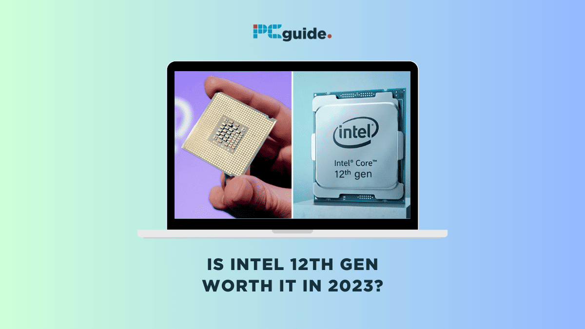
Alder Lake represents Intel’s 12th generation of Core processors, introducing a hybrid architecture that combines Golden Cove performance cores and Gracemont efficient cores. These two core types offer significant advancements over Tiger Lake processors. The Golden Cove performance cores, also known as “P-cores,” incorporate several key improvements.
They feature dedicated floating-point adders, a new 6-wide instruction decoder, a substantial boost in execution ports, and an expanded reorder buffer with 512 entries, enhancing their ability to handle complex tasks efficiently.
While AVX-512 is present, it’s disabled by default to match the E-cores, although it can be manually enabled on some early motherboard BIOS versions.
Alder Lake also brings forth Intel Thread Director. It is a hardware technology aimed at improving load distribution between the heterogeneous P and E cores. This feature requires operating system support to be fully enabled. Additionally, Alder Lake introduces architectural advancements such as last branch records (LBRs), hypervisor-managed linear address translation (HLAT), and Control-flow enforcement technology (CET).
Alder Lake introduces architectural changes to the I/O and memory support as well. It features the LGA 1700 socket for desktop processors.
The 12th-generation processor brought a significant performance boost. At the top was the Intel Core i9-12900K, with 5.3 GHz clock speed and 16 processors. Behind that was the Intel Core i7-12700K, with 4.9 GHz and 12 processors.
Intel 13th gen Core i-series CPUs – Raptor Lake
The codename of the 13th-generation Core i-series processors is Raptor Lake. One of the most notable improvements in Raptor Lake processors is the introduction of a hybrid architecture that combines Raptor Cove performance cores and Gracemont efficiency cores. This hybrid design allows for up to 24 cores and 32 threads, offering exceptional multithreaded and single-threaded performance. The 12th-generation processors had already introduced a hybrid architecture, but Raptor Lake builds upon this with enhanced efficiency and power.
Raptor Lake also benefits from the Intel 7 process, leading to improved power efficiency and overall performance. This new architecture features up to 8 performance cores and 16 efficiency cores.
Moreover, the GPU performance has seen an upgrade with up to 96 Execution Units. This helps process tasks with better speed and efficiency. It also boasts the Intel Iris Xe-LP microarchitecture, providing better graphics capabilities for integrated graphics.
In terms of memory support, Raptor Lake processors are compatible with DDR5-5600 and DDR4, offering faster and more extensive memory options. The chipset improvements, including up to 28 PCI Express lanes and USB 3.2 20 Gbit/s ports, enhance connectivity and data transfer speeds.
Intel 14th gen Core i-series CPUs – Raptor Lake Refresh / Meteor Lake
The Intel 14th-generation Core i-series CPUs are given two different codenames. The first one is Meteor Lake, which was the initial name chosen for the CPUs. However, some CPUs are also codenamed Raptor Lake Refresh due to their similar architecture. That's because the 14th gen continues with the same LGA 1700 socket as the 12th and the 13th gen processors.
Additionally, the number of cores is also the same, except for a few CPUs where the number of efficiency cores has increased slightly to improve performance.
The Raptor Lake Refreshes are released for computers and laptops, whereas the initial releases for Meteor Lake processors are designed for smartphones. However, Intel has confirmed that Meteor Lake processors will come to PCs, too.
Despite the resemblance, Intel’s 14th Gen Core i-series processors represent a significant leap forward in CPU architecture and feature enhancements. One of the most notable changes is the adoption of Intel’s new Foveros advanced packaging technology.
This technology enables the creation of complex chip designs with individual tiles manufactured across multiple process nodes. Therefore, it results in lower power consumption and higher wafer yields. The disaggregation of core components into separate tiles allows for more efficient power usage and improved customizability.
Intel has integrated its Arc GPU architecture, promising up to 2x the performance of previous Iris Xe GPUs. This positions Intel as a more serious competitor in the graphics category. But what's more, is that it opens up the possibility of running AAA games on an internal Intel GPU with hardware-accelerated ray tracing and support for modern enhancements like DirectX 12 Ultimate. The use of Xe super sampling (XeSS) and variable rate shading adds to the appeal of gaming and creative applications.
Furthermore, Meteor Lake brings improvements in power efficiency and battery life for laptops. The updated Thread Director efficiently manages P-cores and E-cores, while features like Intel Intelligent Display automatically adjust display refresh rates and brightness levels.
Which Intel generation is best?
We can say that Intel's 13th-generation processors are the best because of technical advances. They feature more processors than the previous generations. Moreover, they also have better clock speeds.
Although some 14th-generation processors have been released, they are still new to determine whether they are better than 13th-generation processors or not. Therefore, we will go with Raptor Lake processors. However, even 12th-generation processors are not bad. In fact, Core i9 12900K, Core i9 12900KS, and Core i7 12700K are some of the most popular CPUs out there.
Conclusion
Intel’s journey through the Core i-series represents a remarkable story of technological evolution. Each generation brought innovations, performance improvements, and power efficiency enhancements.
This journey will continue for several years. In fact, Intel has already provided some details of its next-gen processors. For one, the 15th-generation processor will be called Arrow Lake. They will feature a different socket than the LGA 1700 that the previous few generations have stuck to.


