A reported leak for the upcoming Intel Lunar Lake CPU prototype has been circulating which reveals an interesting configuration for the chipset over its hybrid architecture predecessors.
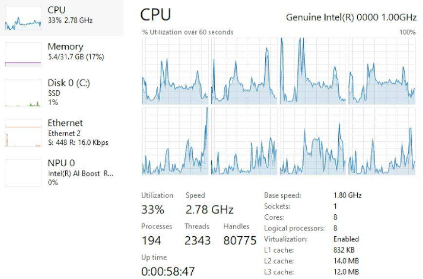
First revealed in a now deleted post on the Zhihu forums, the screenshot showing the alleged Intel Lunar Lake CPU in action has been achieved by the r/hardware subreddit and the results demonstrate just how different Intel Lunar Lake could be from the likes of Raptor Lake and Alder Lake before it, namely in its efficiency.
The A1 sample present is running with a base clock speed of 1.80 GHz complete with eight cores and eight threads meaning that there’s no hyperthreading happening here. There’s also a boost clock of 2.80 GHz, too. Interestingly, there appears to be a higher amount of L2 cache on the chip with 14MB as opposed to L3 cache at 12MB, which goes against the trend we’ve seen from manufacturers investing more heavily into the latter with recent processor generations.

It’s a big departure from the previous hybrid architecture chipsets in terms of their core design. Raptor Lake and Alder Lake before it were forged with both performance cores and efficiency cores clocked differently to seamlessly aid both low-end and more taxing processes at the same time. The lack of any real L1 cache means the company may not be using lower powered efficiency cores with this hardware. There’s a possibility Task Manager could have gotten this wrong, however, as Tom’s Hardware speculates.
This speaks to the heart of what Intel Lunar Lake is expected to be as a lower-end mobile chipset generation based all around efficiency instead of raw power. With seemingly no hyperthreading in action and a low amount of L3 cache, it remains to be seen exactly how this chipset generation could be utilized, especially as it is allegedly releasing later this year. It appears to be consistent with technical details revealed on Guru3D. We could see a much greater focus on the NPU this time around.


